 |
 |
 |
 "What is
Physics Good For?"
"What is
Physics Good For?"
Extra credit is available at the end of this page. Please respond before 9 AM, Monday, November 6th, 2000.
Not very long ago, this was a truism of modern science: "we know atoms exist, but we can never see them." That was before 1982. In that year, Gerd Binnig and Heinrich Rohrer published their first work on a new device known as the Scanning Tunneling Microscope, or STM for short. In 1986, they were awarded the Nobel Prize in physics for their work. This article will describe this breakthrough that has at last allowed us to "see" atoms. I have kept the term "see" in quotes, because the microscope in question does not operate by bouncing light off a sample and creating a magnified image. Rather, the STM operates by taking advantage of quantum tunneling to measure the the shape of the electron "cloud" at the surface of a material. That is, it makes a contour map of the surface, where the contours follow lines of constant electron density. Some people will argue that this is not really "seeing", but there can be little doubt that the peaks and valleys on many STM images represent individual atoms and the spaces between them. How does this amazing device work? The key is in
quantum tunneling. Tunneling is an essential
feature of quantum mechanics, that we can
understand in terms of Heisenberg's uncertainty
principle. In one form, the uncertainty principle
says 
We can interpret this to mean that the energy of a particle can increase for a short period of time, even if the energy does not come from the particle's surroundings. That is, for short periods of time, energy is not conserved. The implications of this notion are astounding. In the case of tunneling, the particle briefly "borrows" an extra bit of energy from nowhere, uses it to travel through a barrier and then gives the enrgy back after it is done. Once the process is done, the particle has it's original energy back, but it now is on the other side of the barrier.
It would be a shame to leave you with the
impression that STM is a scientific curiosity with
no purpose beyond making pretty pictures. On the
contrary, STM is a powerful tool for learning new
and useful information about the physics and
chemistry of surfaces. One example is in the
understanding of how films of materials grow. Many
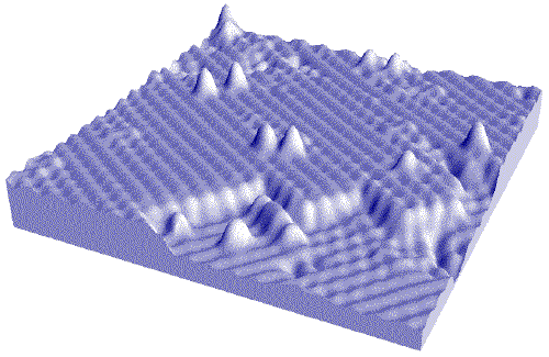
important technologies (semiconductors The figure to the left shows an example (courtesy of Dr. J. Stroscio of the National Institute for Standards and Technology). In these images we do not see the individual atoms laterally, but we do see single atom changes in height. The brightness represents the height of the surface, brighter areas are higher than dark. Thus, the film on the left (a) has grown as many small islands, and there are at least three separate layers showing. On the other hand, the film on the right (b) is growing in a "layer-by-layer" mode. This is desirable because the resulting film will be flatter and have fewer defects. Furthermore, if it is necessary to grow another film on top, the next film will have a better surface to start from, and there may be less intermixing. What allowed the improvement? The only difference was the temperature during film growth. Film (a) was grown at 488 K, whereas film (b)t was grown at 573 K. Films grown at lower temperatures are even worse than (a), and growth above 573 K causes other problems. Thus, an optimum temperature was obtained, along with a clear understanding of the reason.
You can get a lot more information about this subject on the internet. Here are a few search enginesAnd here are a few good links to get you started. You can read more about STM's... From the manufacturers of STM's... And those guys at IBM really go all out... Research Questions (1 point extra credit each!)
This site is made possible by
funding from the National Science Foundation
(DUE-9981111). |
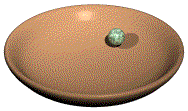 Here is an analogy. A marble is placed in a cereal
bowl and given enough of a push to roll half way up
the side. If there is little friction, the ball can
roll back and forth for a while, but it will never
have enough energy to roll all the way up and over
the wall. It cannot overcome the barrier. However,
for a subatomic particle, the situation is very
different. The particle's energy is tiny, and so
are the barriers it faces. There is a reasonable
chance that a subatomic particle can pass over a
barrier and escape. Once it is out, it doesn't need
the enrgy anymore.
Here is an analogy. A marble is placed in a cereal
bowl and given enough of a push to roll half way up
the side. If there is little friction, the ball can
roll back and forth for a while, but it will never
have enough energy to roll all the way up and over
the wall. It cannot overcome the barrier. However,
for a subatomic particle, the situation is very
different. The particle's energy is tiny, and so
are the barriers it faces. There is a reasonable
chance that a subatomic particle can pass over a
barrier and escape. Once it is out, it doesn't need
the enrgy anymore.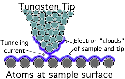 This is how the scanning tunneling microscope
works. In the STM, a very sharp metal tip (usually
tungsten) is held near the surface of a conducting
sample. A small valtage (usually 1.5 to 3 V) is
placed between the tip and the sample. Now, the
electrons in the tip would like to flow to the
sample. If the tip touches the sample current will
flow easily, if the tip is far away, the electrons
cannot overcome the barrier and "jump" the gap.
However, if the distance is just right, the
electrons can tunnel out of the tip and get into
the sample. This process is illustrated in the
diagrams.
This is how the scanning tunneling microscope
works. In the STM, a very sharp metal tip (usually
tungsten) is held near the surface of a conducting
sample. A small valtage (usually 1.5 to 3 V) is
placed between the tip and the sample. Now, the
electrons in the tip would like to flow to the
sample. If the tip touches the sample current will
flow easily, if the tip is far away, the electrons
cannot overcome the barrier and "jump" the gap.
However, if the distance is just right, the
electrons can tunnel out of the tip and get into
the sample. This process is illustrated in the
diagrams.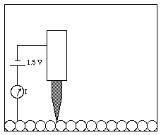 What makes this process truly wonderful (besides
the fact that it can happen at all) is the
tunneling current depends very sensitively on the
size of the gap. If we move the tip laterally over
the sample, the current changes strongly in
response to variations in the surface height. This
is known as constant height mode. What is actually
even better is constant current mode. In this
operation, the tip is moved laterally, and as it
moves its height is adjusted in order to keep the
tunneling current constant. As this process occurs,
the height adjustments are recorded. The tip
literally follows the contours of the sample.
What makes this process truly wonderful (besides
the fact that it can happen at all) is the
tunneling current depends very sensitively on the
size of the gap. If we move the tip laterally over
the sample, the current changes strongly in
response to variations in the surface height. This
is known as constant height mode. What is actually
even better is constant current mode. In this
operation, the tip is moved laterally, and as it
moves its height is adjusted in order to keep the
tunneling current constant. As this process occurs,
the height adjustments are recorded. The tip
literally follows the contours of the sample.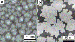 and magnetic
storage come to mind) depend on devices that are
made of thin films of material (silicon and
magnetic alloys in those two examples). The
precision of the devices depends crucially on the
precision with which the films can be grown. STM
has helped to solve many problems in our
understanding of film growth.
and magnetic
storage come to mind) depend on devices that are
made of thin films of material (silicon and
magnetic alloys in those two examples). The
precision of the devices depends crucially on the
precision with which the films can be grown. STM
has helped to solve many problems in our
understanding of film growth.